TiW alloy adhesion layer for integration of anodic aluminum oxide on substrates
A method for developing an integrated via structure for improved performance in CMOS applications at millimeter- and submillimeter-wave frequencies

Applications
- Submillimeter-Wave Communications
- Millimeter-Wave Communications
- Internet of Things Devices
- 3D integrated circuits
Technology Overview
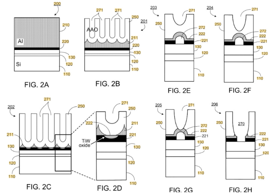
In IC circuits and systems, vias play a significant role in providing high-density interconnections between active devices, however, as the communication frequency band expands progressively into millimeter and even submillimeter-wave frequencies, higher skin depth loss and parasitic inductance for vias become prohibitive. Researchers at the University of Minnesota have developed a method for using a TiW adhesion layer to integrate anodic aluminum oxide (AAO) on substrates, removing the commonly formed barrier layer for electrical contact, and widening the pores of the AAO for various nanomaterials and devices. Using this structure, bundles of nanowires are fabricated in an ultrathin device, resulting in a decrease in total power loss at high frequencies with improved integration.
Phase of Development
TRL: 4Working prototypes have been developed.
Desired Partnerships
This technology is now available for:- License
- Sponsored research
- Co-development
Please contact our office to share your business’ needs and learn more.
Press Releases
University of Minnesota College of Science & Engineering January 29, 2021Researchers
- Bethanie Stadler Professor, Electrical and Computer Engineering
- Rhonda Franklin Professor, Department of Electrical and Computer Engineering
-
expand_more library_books References (1)
- Yali Zhang; Joseph Um; Bethanie Stadler; Rashaunda Henderson; Rhonda Franklin (2021), Study of Nanowire-Based Integrated via Technology for CMOS Application in Millimeter-Wave Frequencies, IEEE Microwave and Wireless Components Letters, 31, 693 - 696
-
expand_more cloud_download Supporting documents (1)Product brochureTiW alloy adhesion layer for integration of anodic aluminum oxide on substrates.pdf